

Silicon Patterns is Building the Engineering Backbone of India’s Semiconductor Revolution
The World Needs More Chip Engineers. India Has Them.
The global semiconductor industry is hurtling toward a historic milestone — a $1 trillion market by the end of 2026, driven almost entirely by an insatiable demand for AI-optimised silicon. Hyperscalers like Amazon, Microsoft, Google, and Meta have collectively committed over $660 billion in capital expenditure this year alone. Custom chip architectures — from AI accelerators to edge inference processors — are no longer a future aspiration; they are a present-day business imperative.
Yet beneath this gold rush lies a crisis that threatens to derail it. A deepening, structural shortage of qualified chip design engineers is slowing the world’s most critical technology build-out. The United States graduates fewer than 100,000 students annually in computer science and electrical engineering combined. Europe faces an aging talent base. By 2030, industry analysts project a global deficit of over one million semiconductor specialists.
India, meanwhile, is sitting on the world’s largest and fastest-growing pool of chip design talent — accounting for an estimated 20% of the global semiconductor engineering workforce. The question is no longer whether India can solve the global chip talent crisis. The question is whether Indian companies will rise to the moment and build the institutional capacity to deliver at the world’s highest standards.
Silicon Patterns, the Hyderabad-based semiconductor engineering services company founded in 2022, is betting that the answer is yes — and building the proof.
Leadership Speaks: The CEO’s Vision
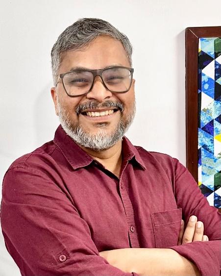
Srinivasa Gupta Cheedella, Co-Founder & CEO, Silicon Patterns ,IIT Madras · Ex-HARMAN International
” The global AI boom is not just a software story — it is a silicon story. And the silicon story cannot be written without India’s engineers. We built Silicon Patterns because we believed India’s deep engineering talent, paired with world-class processes, could contribute something lasting to how the world designs chips.
— Srinivasa Gupta Cheedella, Co-Founder & CEO, Silicon Patterns
A Master of Science graduate from the Indian Institute of Technology (IIT) Madras, Cheedella spent years shaping embedded systems and chip design strategy at HARMAN International before co-founding Silicon Patterns. His thesis was simple but audacious: India did not need to wait for a fab to become a global semiconductor power. It already had what the world needed most — elite design engineering talent. What it lacked was a world-class delivery platform to channel that talent toward the most complex and consequential chips being built today.
“When a global AI company needs a chip that processes inference at the edge in under one millisecond, the engineering behind that requires people who live and breathe silicon,” says Cheedella. “We are building that team in India — and the world is coming to us.”
The Co-Founder’s Perspective: Engineering at the Frontier
Prasanna Kumar Thadapaneni,Co-Founder & Director, Silicon Patterns, Ex Soctronics
“India has always produced brilliant chip designers. What was missing was an organisation willing to take on the hardest problems — HBM3, AI silicon, automotive-grade verification — and deliver them at the quality global clients expect. That is exactly what we set out to build. The talent shortage the world is worried about? We are solving it, one tapeout at a time.”
— Prasanna Kumar Thadapaneni, Co-Founder & Director, Silicon Patterns
Prasanna Kumar Thadapaneni brings to Silicon Patterns a career built at the deepest levels of chip design. Invecas group of companies— the global leader in mobile chipsets — and Soctronics, Thadapaneni’s expertise spans physical design, timing closure, and Design for Testability (DFT), among the most technically demanding disciplines in the semiconductor world. As Co-Founder and Director, he oversees the company’s engineering delivery and quality frameworks.
“Chip design is one of the last domains in engineering where you cannot fake depth,” he notes. “A bug in RTL that reaches silicon can cost a client six months and tens of millions of dollars. The culture we have built at Silicon Patterns reflects the gravity of that responsibility. We do not hire for scale — we hire for depth.”
The Crisis in Numbers: Why the World Cannot Afford to Ignore India
The scale of the global chip talent crisis is difficult to overstate. According to Deloitte, by 2030 the semiconductor industry’s talent deficit will exceed one million specialists worldwide — a shortage that no amount of reshoring investment or policy incentive can fix without a radically expanded global talent base.
AI is the accelerant. AI chips, which represent just 0.2% of all chips manufactured, now account for roughly 50% of total semiconductor industry revenue. The economics of custom silicon have never been more compelling — or the engineering demands more exacting. Designing an AI accelerator for a hyperscaler’s data centre requires expertise in RTL design, SystemC modelling, HBM3/3E memory interfaces, physical design, design verification, and post-silicon validation — simultaneously. Very few engineering organisations in the world can credibly execute across all of these disciplines.
Silicon Patterns can. Its end-to-end capability stack — spanning RTL Design, SystemC Modelling, Emulation, Design Verification (DV), Physical Design (PD), Design for Testability (DFT), and Pre- & Post-Silicon Validation — covers the full chip development lifecycle. Its domain expertise in Wireless, IoT, Automotive, AI/ML, and advanced HBM3/3E workloads positions it precisely at the intersection of where the industry’s hardest problems are being solved today.
SILICON PATTERNS — END-TO-END CAPABILITIES
- RTL Design & SystemC Modelling — the blueprint of every chip
- Emulation & Design Verification (DV) — catching bugs before silicon
- Physical Design (PD) — translating logic into manufacturable layouts
- Design for Testability (DFT) — ensuring every chip can be tested at scale
- Pre- & Post-Silicon Validation — from first silicon to production-ready
- Domains: AI/ML · Automotive · Wireless · IoT · HBM3/3E · Edge Computing
Engagement Models: T&M · ODC · Subcontracting · Build-Operate-Transfer (BOT)
India’s Semiconductor Moment — And Why It Cannot Be Wasted
India’s policy environment has never been more aligned with Silicon Patterns’ mission. The government’s India Semiconductor Mission (ISM) has committed ₹76,000 crore in incentives, 10 semiconductor projects with cumulative investments exceeding ₹1.60 lakh crore have been approved across six states, and the ISM 2.0 roadmap targets 3-nanometer and 2-nanometer chip design capabilities by 2035. India has inaugurated its first advanced 3nm chip design centres. By 2029, India aims to design and manufacture chips covering 70–75% of domestic applications.
For Silicon Patterns, this policy tailwind is validation not a dependency. The company was built to be globally competitive from day one, with offices in Hyderabad, Bangalore, Raipur, and Noida, and a delivery model designed to serve clients in the United States, Europe, and Asia-Pacific. The ISM’s ambition aligns with what Silicon Patterns is already executing: the creation of world-class chip design capacity on Indian soil.
“India’s moment in semiconductors is not a government talking point it is an engineering reality,” says CEO Srinivasa Gupta Cheedella. “The talent is here. The policy is here. The global demand is here. What Indian companies like ours must now do is deliver at the highest level, every single time.”
“The $1 trillion chip market is not going to be built by any single country or company. It is going to be built by networks of engineering excellence. India — and Silicon Patterns — must be at the centre of that network.”
— Srinivasa Gupta Cheedella, Co-Founder & CEO, Silicon Patterns
Looking Ahead: Solving the Crisis, One Chip at a Time
Silicon Patterns’ roadmap is defined by three strategic priorities. First, deepening expertise in AI silicon the fastest-growing and most demanding segment of the semiconductor market including HBM3/3E-integrated AI accelerators, edge inference processors, and GenAI/LLM-optimised chip architectures. Second, expanding its global client base, targeting fabless design houses and AI-native technology companies that need engineering partners capable of executing across the full chip development lifecycle. Third, building India’s next generation of chip design engineers not just hiring them, but developing the deep specialisation that the industry’s hardest problems demand.
“The global chip talent crisis is real,” acknowledges Co-Founder Prasanna Kumar Thadapaneni. “But it is also an extraordinary opportunity for India. Every engineer we train, every tapeout we deliver, every client relationship we build that is India’s answer to the crisis. Chip by chip, engineer by engineer, we are writing India’s semiconductor story.”
The world’s AI ambitions run on silicon. Silicon runs on engineering talent. And that engineering talent, increasingly, runs through India and through companies like Silicon Patterns that are building the infrastructure of excellence that the global chip industry needs.
ABOUT SILICON PATTERNS The global AI boom is not just a software story — it is a silicon story. And the silicon story cannot be written without India’s engineers. We built Silicon Patterns because we believed India’s deep engineering talent, paired with world-class processes, could contribute something lasting to how the world designs chips.
Silicon Patterns Private Limited is a Hyderabad-headquartered semiconductor engineering services company founded in October 2022. The company delivers end-to-end semiconductor and embedded system engineering services spanning RTL Design, SystemC Modelling, Emulation, Design Verification (DV), Physical Design (PD), Design for Testability (DFT), and Pre- & Post-Silicon Validation. With deep expertise in AI/ML chip design, HBM3/3E workloads, Automotive, Wireless, and IoT domains, Silicon Patterns serves global clients through flexible engagement models including Time & Materials (T&M), Offshore Development Centers (ODC), Subcontracting, and Build-Operate-Transfer (BOT). The company operates from offices in Hyderabad, Bangalore, Raipur, and Noida.
CONNECT WITH SILICON PATTERNS
Website: https://www.siliconpatterns.com
Services: https://www.siliconpatterns.com/services
About Us: https://www.siliconpatterns.com/about